| 基本投资额 | 大于100万元 |
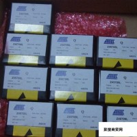
| 品牌 | ACTEL |
| 型号 | A54SX32A-CQ208B |
The AT84AD001B is a mo
nolithic dual 8-bit analog-to-digital converter, offering low
1.4W power co
nsumption and excellent digitizing accuracy. It integrates dual on-chip
track/holds that provide an enhanced dynamic performance with a sampling rate of up to
1 Gsps an**nput frequency bandwidth of over 1.5 GHz. The dual concept, the integrated
demultiplexer and the easy interleaving mode make this device user-friendly for
all dual channel applications, such as direct RF co
nversion or data acquisition. The
smart function of the 3-wire serial interface eliminates the need for external components,
which are usually necessary for gain and offset tuning and setting of other
parameters, leading to space and power reduction as well as system flexibility.The AT84AD001B is a dual 8-bit 1 Gsps ADC ba
sed on advanced high-speed
BiCMOS technology.
Each ADC includes a front-end analog multiplexer followed by a Sample and Hold (S/H),
and an 8-bit flash-like architecture core analog-to-digital converter. The output data is
followed by a switchable 1:1 or 1:2 demultiplexer and LVDS output buffers (100Ω).
Two over-range bits are provided for adjustment of the external gain co
ntrol on each
channel.
A 3-wire serial interface (3-bit address and 16-bit data) is included to provide several
adjustments:
• Analog input range adjustment (±1.5 dB) with 8-bit data co
ntrol using a 3-wire bus
interface (steps of 0.18 dB)
• Analog input switch: both ADCs can co
nvert the same analog input signal I or Q
• Gray or binary encoder output. Output format: DMUX 1:1 or 1:2 with co
ntrol of the
output frequency on the data ready output signal
• Partial or full standby on channel I or channel Q
• Clock selec
tion:
– Two independent clocks: CLKI and CLKQ
– One master clock (CLKI) with the same phase for channel I and channel Q
– One master clock but with two phases (CLKI for channel I and CLKIB for
channel Q)
• ISA: Internal Settling Adjustment on channel I and channel Q
• FiSDA: Fine Sampling Delay Adjustment on channel Q
• Adjustable Data Ready Output Delay on both channels
• Test mode: decimation mode (by 16), Built-In Test.
A calibration phase is provided to set the two DC offsets of channel I and channel Q
close to code 127.5 and calibrate the two gains to achieve a maximum difference of
0.5 LSB. The offset and gain error can also be set externally via the 3-wire serial
interface.
The AD84AD001B operates in fully differential mode from the analog inputs up to the
digital outputs. The AD84AD001B features a full-power input bandwidth of 1.5 GHz.


 微信客服
微信客服 微信公众号
微信公众号 查看详情
查看详情 查看详情
查看详情 查看详情
查看详情 查看详情
查看详情 查看详情
查看详情 查看详情
查看详情


 查看详情
查看详情 查看详情
查看详情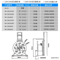 查看详情
查看详情 查看详情
查看详情 查看详情
查看详情 查看详情
查看详情 查看详情
查看详情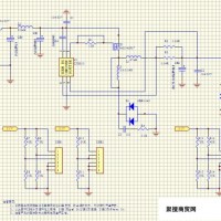 查看详情
查看详情 查看详情
查看详情 查看详情
查看详情